Harnessing the power of the sun and creating light-harvesting or light-sensing devices requires a material that both absorbs light efficiently and converts the energy to highly mobile electrical current. Finding the ideal mix of properties in a single material is a challenge, so scientists have been experimenting with ways to combine different materials to create "hybrids" with enhanced features.
In two just-published papers, scientists from the U.S. Department of Energy's Brookhaven National Laboratory, Stony Brook University, and the University of Nebraska describe one such approach that combines the excellent light-harvesting properties of quantum dots with the tunable electrical conductivity of a layered tin disulfide semiconductor. The hybrid material exhibited enhanced light-harvesting properties through the absorption of light by the quantum dots and their energy transfer to tin disulfide, both in laboratory tests and when incorporated into electronic devices. The research paves the way for using these materials in optoelectronic applications such as energy-harvesting photovoltaics, light sensors, and LEDs.

|
|
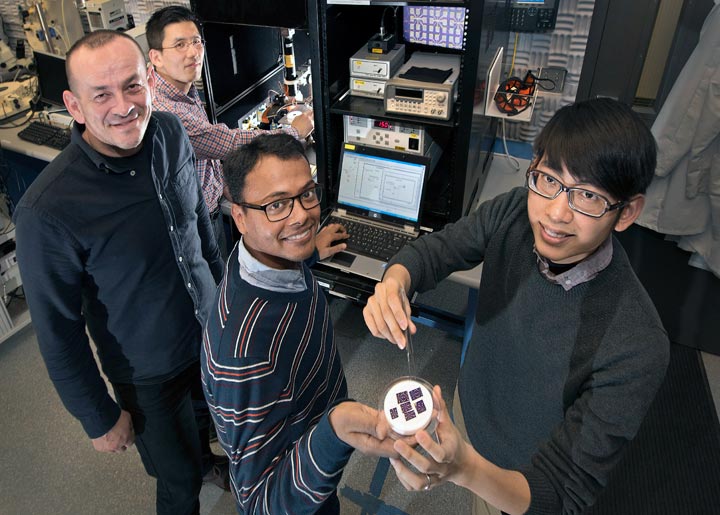
The research team at a probe station where they used simulated sunlight to characterize electronic devices they'd made using a hybrid nanomaterial (back to front: Chang-Yong Nam and Mircea Cotlet of Brookhaven Lab's Center for Functional Nanomaterials with Stony Brook University graduate students Prahlad Routh and Jia-Shiang Chen).
|
According to Mircea Cotlet, the physical chemist who led this work at Brookhaven Lab's Center for Functional Nanomaterials, a DOE Office of Science User Facility, "Two-dimensional metal dichalcogenides like tin disulfide have some promising properties for solar energy conversion and photodetector applications, including a high surface-to-volume aspect ratio. But no semiconducting material has it all. These materials are very thin and they are poor light absorbers. So we were trying to mix them with other nanomaterials like light-absorbing quantum dots to improve their performance through energy transfer."
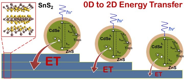
One paper, just published in the journal ACS Nano, describes a fundamental study of the hybrid quantum dot/tin disulfide material by itself. The work analyzes how light excites the quantum dots (made of a cadmium selenide core surrounded by a zinc sulfide shell), which then transfer the absorbed energy to layers of nearby tin disulfide.
"We have come up with an interesting approach to discriminate energy transfer from charge transfer, two common types of interactions promoted by light in such hybrids," said Prahlad Routh, a graduate student from Stony Brook University working with Cotlet and co-first author of the ACS Nano paper. "We do this using single nanocrystal spectroscopy to look at how individual quantum dots blink when interacting with sheet-like tin disulfide. This straightforward method can assess whether components in such semiconducting hybrids interact either by energy or by charge transfer."

|
|
Single nanocrystal spectroscopy identifies the interaction between zero-dimensional CdSe/ZnS nano crystals (quantum dots) and two-dimensional layered tin disulfide as a non-radiative energy transfer, whose strength increases with increasing number of tin disulfide layers. Such hybrid materials could be used in optoelectronic devices such as photovoltaic solar cells, light sensors, and LEDs.
|
The researchers found that the rate for non-radiative energy transfer from individual quantum dots to tin disulfide increases with an increasing number of tin disulfide layers. But performance in laboratory tests isn't enough to prove the merits of potential new materials. So the scientists incorporated the hybrid material into an electronic device, a photo-field-effect-transistor, a type of photon detector commonly used for light sensing applications.
As described in a paper published online March 24 in Applied Physics Letters, the hybrid material dramatically enhanced the performance of the photo-field-effect transistors—resulting in a photocurrent response (conversion of light to electric current) that was 500 percent better than transistors made with the tin disulfide material alone.
"This kind of energy transfer is a key process that enables photosynthesis in nature," said Chang-Yong Nam, a materials scientist at Center for Functional Nanomaterials and co-corresponding author of theAPL paper. "Researchers have been trying to emulate this principle in light-harvesting electrical devices, but it has been difficult particularly for new material systems such as the tin disulfide we studied. Our device demonstrates the performance benefits realized by using both energy transfer processes and new low-dimensional materials."
Cotlet concludes, "The idea of 'doping' two-dimensional layered materials with quantum dots to enhance their light absorbing properties shows promise for designing better solar cells and photodetectors."
Former Brookhaven Lab staff members Huidong Zang, Huang Yuan, Eli Sutter, and Peter Sutter, and Jia-Shiang Wang, a Stony Brook University graduate student with working with Cotlet, also contributed to this work. The research was funded by the DOE Office of Science.
Brookhaven National Laboratory is supported by the Office of Science of the U.S. Department of Energy. The Office of Science is the single largest supporter of basic research in the physical sciences in the United States, and is working to address some of the most pressing challenges of our time. For more information, please visit science.energy.gov.
Related Links


